**ADP5023ACPZ-2-R7: A Comprehensive Technical Overview and Application Guide**
The **ADP5023ACPZ-2-R7** from Analog Devices is a highly integrated, dual-channel, step-down (buck) regulator with a low-dropout linear regulator (LDO), designed to meet the complex power management requirements of modern electronic systems. This monolithic IC is particularly suited for space-constrained applications such as portable instrumentation, medical devices, and communication infrastructure, where high efficiency, minimal footprint, and reliable performance are paramount.
**Architectural Overview and Key Specifications**
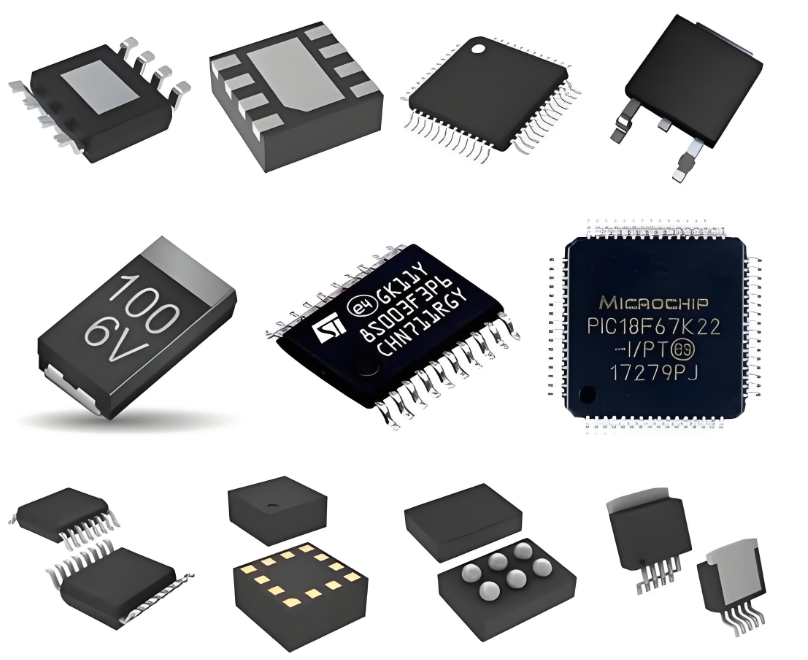
At its core, the ADP5023 combines two high-performance, synchronous buck regulators and one LDO in a single 24-lead LFCSP package. The two buck converters are capable of delivering up to **1.2 A and 0.6 A of output current** respectively. They operate at a fixed switching frequency of **3 MHz**, which allows for the use of exceptionally small external inductors and capacitors, significantly reducing the overall solution size. The high switching frequency also enables excellent transient response to rapid changes in load current.
The integrated LDO can supply up to **200 mA of output current** and offers a low dropout voltage, making it ideal for powering noise-sensitive circuitry like phase-locked loops (PLLs) or analog sensors from one of the buck converter outputs. A key feature of the ADP5023 is its **wide input voltage range of 2.85 V to 5.5 V**, making it perfectly compatible with common system rails such as 3.3 V or 5 V, as well as lithium-ion batteries.
**Critical Features and Performance Advantages**
* **High Efficiency Operation:** The buck regulators utilize a synchronous rectification architecture to minimize power loss. Efficiency peaks well above **90%**, which is critical for battery-powered devices to extend operational life and manage thermal dissipation.
* **Precision Output Voltage:** The output voltages for all three regulators are user-adjustable via external resistors. The bucks can be set from **0.8 V to 3.8 V**, while the LDO can be adjusted from **1.0 V to 3.8 V**, providing flexibility for powering a wide array of low-voltage ICs like FPGAs, ASICs, and microprocessors.

* **Advanced Control and Protection:** The device includes a comprehensive suite of protection features, including **undervoltage lockout (UVLO), overcurrent protection (OCP), and thermal shutdown (TSD)**. These features safeguard the IC and the downstream load under fault conditions. The **power-good (PG) output** signal provides a status monitor for system-level power sequencing.
* **Low Quiescent Current:** In light-load conditions, the buck regulators automatically enter a pulse-frequency modulation (PFM) mode to maintain high efficiency, thereby reducing the **quiescent current** and conserving power.
**Application Guide and Design Considerations**
Implementing the ADP5023 requires careful attention to the layout and selection of external components to achieve optimal performance.
1. **Input Capacitor (CIN):** Place a **low-ESR ceramic capacitor** as close as possible to the PVINx and PGND pins of each buck regulator. A value of **4.7 µF to 10 µF** is typically recommended to filter high-frequency switching noise and provide localized charge.
2. **Output Capacitor (COUT):** The stability and transient response of the buck regulators are heavily dependent on the output capacitor. Use X5R or X7R dielectric ceramic capacitors with a typical total value of **10 µF to 22 µF**.
3. **Inductor Selection:** For each buck channel, select an inductor with a low DC resistance (DCR) to minimize I²R losses. The inductance value is determined by the desired ripple current; a value between **0.47 µH and 1.5 µH** is common for the 3 MHz operation. Ensure the inductor’s saturation current rating exceeds the peak switch current limit.
4. **Layout Prioritization:** A proper PCB layout is non-negotiable for switching regulators. **Keep the high-current loops (CIN → Buck → L → COUT) as small and tight as possible**. Use a solid ground plane and ensure the feedback paths (FBx pins) are routed away from noisy switching nodes to avoid noise coupling.
**ICGOODFIND:** The ADP5023ACPZ-2-R7 stands out as an exceptional power management solution, masterfully balancing high integration, superior efficiency, and a miniature footprint. Its robust architecture, combining dual high-frequency bucks and an LDO, simplifies power supply design for advanced systems, making it a top-tier choice for engineers tackling the challenges of modern electronic design.
**Keywords:** Power Management IC (PMIC), Step-Down Regulator, High Switching Frequency, Low Quiescent Current, Integrated LDO.
